Modern computing needs better semiconductor technology for faster performance. A new transistor design has changed how processors are made.
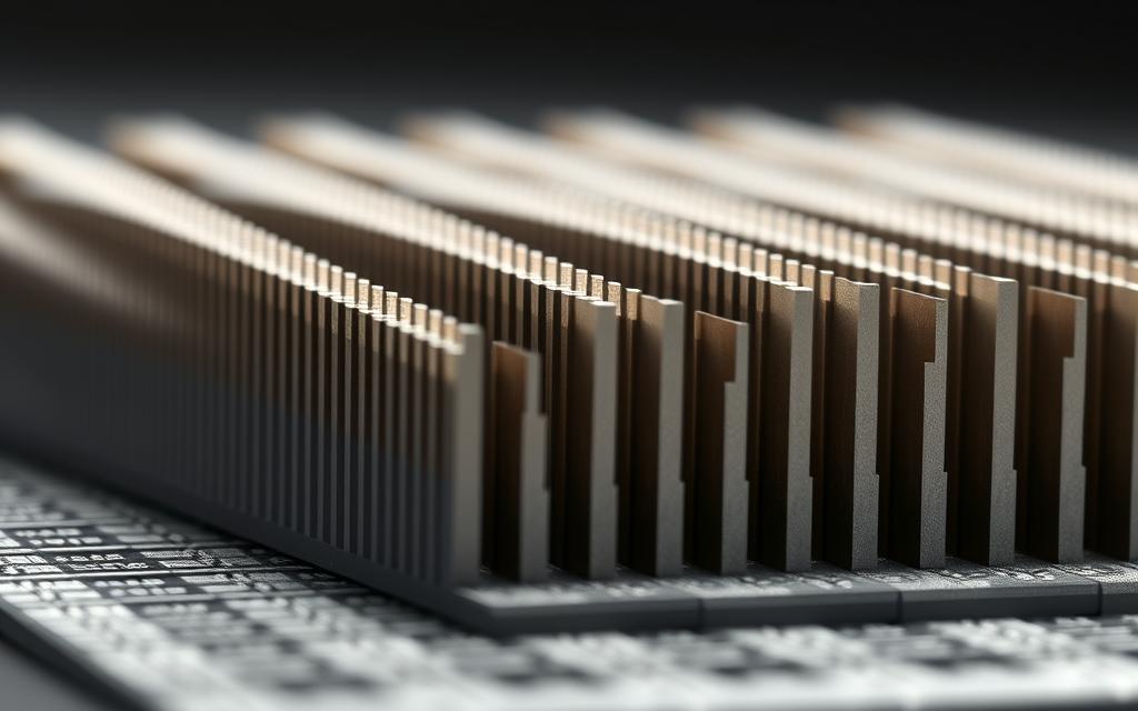
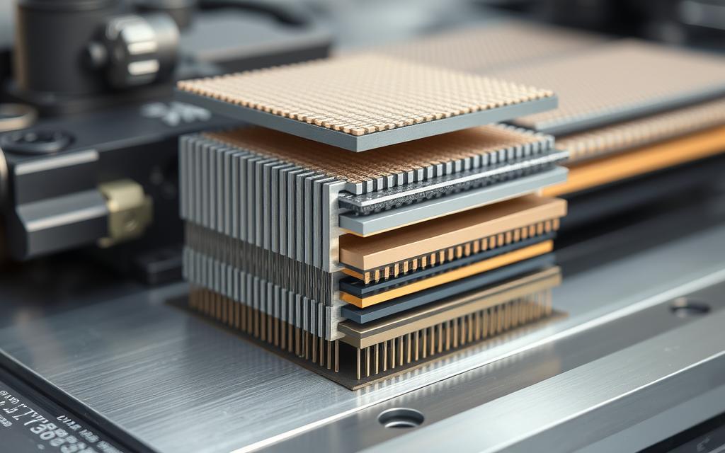
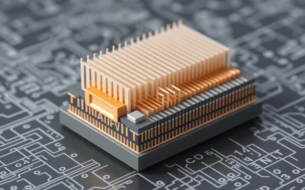
The finfet transistor is a big change from old designs. It has a three-dimensional shape. The gate goes around a raised silicon channel, making a ‘fin’.
This design has big benefits. It makes switching faster and carries more current. It also uses less power.
FinFET is key to today’s modern processors. It’s used in important sizes like 14nm, 10nm, and 7nm.
This technology has changed nanoelectronics. It lets computers get faster and use less energy. This innovation is helping make the latest computing devices.
The Foundation of Modern Semiconductor Technology
When dimensions fell below 28 nanometres, traditional transistors hit a wall. The industry’s drive for smaller sizes hit physical limits. This led to a need for new designs, not just tweaks.
Planar MOSFET Limitations at Nanoscale
At atomic scales, the old planar MOSFET design struggled. It was made for much larger sizes and couldn’t keep up with the new demands.
Gate control over the channel area weakened. This caused short-channel effects, where electrons could jump past the gate. This made transistor performance unpredictable and worse.
Quantum tunnelling became a big problem. Electrons could tunnel through thin barriers, making old designs useless at the atomic level.
The industry reached a point where smaller meant worse performance and more power use. This was a major problem that needed a new approach to transistor design.
The Physical Constraints of Traditional Transistor Design
Scaling transistors faced many physical barriers. Doping levels became too high, causing unstable threshold voltages.
Leakage current was a huge issue. Thin insulators let electrons escape, causing several problems:
- Gate oxide tunnelling current
- Subthreshold leakage through the channel
- Junction leakage at source/drain interfaces
Leakage started to dominate power use, changing how designers worked. This was a big shift from what they were used to.
The table below shows the main challenges at advanced nodes:
| Physical Constraint | Impact at 28nm Node | Impact Below 22nm | Primary Consequence |
|---|---|---|---|
| Gate Control Loss | Moderate performance variation | Catastrophic failure modes | Unpredictable transistor behaviour |
| Quantum Tunnelling | Manageable leakage increase | Dominant leakage mechanism | Exponential power increase |
| Doping Fluctuations | Statistical threshold variation | Complete loss of uniformity | Manufacturing yield collapse |
| Heat Density | Cooling challenges | Localised thermal runaway | Device reliability failure |
The industry needed a new approach to overcome these challenges. It had to solve problems with electrostatics, leakage, and manufacturing all at once.
The move to three-dimensional transistors was a big change. It was necessary to keep scaling and advancing computing.
What Is FinFET Technology
FinFET technology is a big change in how transistors are made. It helps solve problems with old designs. This new way is key for making smaller, better devices.
Architectural Revolution: The Fin Structure
FinFETs have a special three-dimensional fin structure. This fin rises from the silicon base. It lets the gate electrode wrap around, giving better control than flat transistors.
The fins are very thin, just a few nanometres wide. This allows for more devices in the same space. It also helps in making complex circuits without taking up more room.

Gate Control and Channel Formation Mechanisms
FinFETs work better because of how they control the gate. The gate wraps around the fin in a trigate setup. This creates a uniform electric field in the channel.
This design has many benefits:
- It improves control over the channel
- It makes carrier transport more efficient
- It reduces short-channel effects at smaller sizes
- It helps manage the threshold voltage better
The better gate control means the transistor can switch on and off more efficiently. This reduces leakage currents, a big problem with old designs.
Key Differentiators from Planar Transistors
FinFETs are different from planar transistors in many ways. These differences make FinFETs great for high-performance computing.
3D Structure vs Planar Design
FinFETs have a 3D design, unlike flat planar transistors. This design gives more gate control area. It helps improve performance without needing bigger chips.
Superior Electrostatic Control
The wrap-around gate design gives better control over the channel. This reduces leakage currents and makes switching more efficient.
Reduced Body Effect
FinFETs have less body effect than planar transistors. This means the threshold voltage is less affected by voltage changes. It leads to more consistent performance.
As a multigate device, FinFET technology is a big step forward in semiconductor design. It’s key for making devices smaller and better. It’s the top choice for making advanced processors.
Technical Advantages of FinFET Architecture
FinFET technology is a big step forward in making semiconductors. It brings big improvements in many areas. The fin structure changes how transistors work at tiny scales, beating traditional designs.
https://www.youtube.com/watch?v=4fE-dWoNua4
Superior Electrostatic Control
The wrap-around gate design gives electrostatic control over the channel. It lets the gate control the channel from three sides, not just one.
This better control cuts down on short-channel effects. It makes transistors work better and more reliably at smaller sizes.
With better gate control, transistors can switch more reliably at lower voltages. This leads to better performance and less power use.
Power Consumption Reductions
FinFET technology is very good at saving power. It can work at lower voltages without losing performance. This is a big plus.
It means devices can do the same work using less energy. This is great for battery-powered devices where saving power is key.
It also makes power gating more effective. Designers can turn off unused parts of the circuit better, saving even more power.
Performance Enhancement Capabilities
FinFET architectures bring big performance gains. The three-dimensional design lets for more current flow in the same space.
Transistors switch faster, allowing for higher clock speeds. They can also drive larger loads without losing performance. This is thanks to their drive strength.
Designers can use multiple fins per transistor to boost performance even more. This makes it easier to tailor designs for different needs.
Leakage Current Minimisation
Another big plus is leakage minimisation. The wrap-around gate structure helps reduce subthreshold leakage currents. This is a big problem for traditional transistors at small sizes.
Leakage power was often a bigger problem than dynamic power in older technologies. But FinFETs change this.
The better electrostatic control means transistors use less power when not in use. This leads to a big drop in standby power across entire chips.
Manufacturing and Implementation Challenges
Creating FinFET transistors is a complex task. It’s unlike making flat transistors. The three-dimensional design needs precise engineering and new manufacturing methods.
Fabrication Complexities and Solutions
Making the fin structures is a big challenge. The vertical shape needs perfect etching to keep sizes uniform. Small errors can affect how well the transistors work and how many are made.
At smaller sizes, making patterns gets harder. Multi-patterning lithography helps by breaking down the pattern into steps. But, it adds complexity and needs careful alignment.

EUV lithography is a game-changer for making finer patterns. It uses shorter wavelengths than old tools. This means fewer steps are needed, making the process simpler and more accurate.
Companies have found new ways to tackle these problems:
- Advanced etching techniques with atomic-level precision
- Novel materials for better process control
- Enhanced metrology systems for real-time monitoring
- Improved defect detection and correction methodologies
Process Integration Considerations
FinFETs need careful planning to work well. Designers and manufacturers must work together. This ensures designs can be made on a large scale.
Today’s design tools help with this. They consider how things will be made during design. This way, problems are caught early, not at the end.
Designing for manufacturing is key. Engineers must think about how things will vary during production. Tools help predict and adjust for these changes.
Important things to think about include keeping things cool, managing stress, and dealing with unwanted elements. These affect how well the transistors work and how reliable they are. Special tools help understand and improve these issues.
Industry Adoption and Processor Applications
The semiconductor industry has fully adopted FinFET technology, marking a major shift in computing. This change allowed for better performance beyond what planar transistors could offer. Now, FinFETs power everything from smartphones to supercomputers.
Intel’s 22nm Tri-Gate Implementation
Intel was the first to use FinFETs commercially with their 22nm Tri-Gate technology in 2011. This innovation was seen in Ivy Bridge processors, bringing a big jump in density and efficiency. The three-dimensional design greatly improved control over the channel, cutting down leakage current by over 90%.
Intel chose fin heights that balanced performance and manufacturing success. This move made FinFETs the new standard for advanced nodes in the industry.
TSMC’s 16nm and 7nm FinFET Processes
TSMC joined the FinFET market with their 16nm process in 2013. They quickly became key for mobile processors and GPUs. By 2017, they reached 7nm nodes, powering top devices from Apple, Qualcomm, and AMD.
TSMC’s success came from better process integration and design rules. Their FinFETs offered high performance at lower voltages, essential for battery life.
Samsung’s Foundry Technology Roadmap
Samsung Foundry pushed the node race with their 10nm process in 2013. They then hit 5nm in 2018, competing with TSMC for top mobile processor deals.
Samsung focused on improving performance per watt with fin profile tweaks and new gate stack materials. Their work has greatly expanded FinFET use in various devices.
Mobile versus Desktop Processor Implementations
FinFETs are used differently in mobile and desktop processors. Mobile chips focus on saving power with lower voltages and fewer fins. This helps extend battery life.
Desktop and server chips, on the other hand, aim for top performance. They use more fins and higher currents, accepting more power for better speed. This flexibility lets makers design transistors for specific needs.
This shows how FinFETs meet the needs of both power-saving mobile devices and high-performance systems. Their ability to scale continues to drive progress in computing.
Conclusion
FinFET technology has changed how we design processors, making them faster and more efficient. It helped the industry get past old limits and keep improving computers.
Now, FinFETs face big challenges at 5nm and smaller sizes. The problem is leakage current, which gets worse as we get closer to the atomic level. This means we need new ways to make transistors to keep improving.
The next step might be Gate-All-Around FET (GAAFET) technology. It uses nanowires or nanosheets for better control. Companies like Samsung and TSMC are working on GAAFET for future chips.
Keeping Moore’s Law alive is key to this progress. Each new technology builds on the last, keeping computers getting better. Moving from planar to FinFET to GAAFET shows the industry’s drive for better.
The future of transistors will bring even more new ideas as we hit physical limits. We might see new materials and three-dimensional designs. This ongoing journey will keep making computers more powerful for our needs.
FAQ
What is FinFET technology?
FinFET technology uses a three-dimensional transistor design. It has a raised silicon ‘fin’ structure, with the gate wrapped around it. This design improves control over the channel, making it more efficient and powerful than traditional transistors.
Why did the semiconductor industry move beyond planar MOSFETs?
Planar transistors hit limits as they got smaller than 28nm. They had trouble controlling the channel, leading to high leakage currents and power use. Scaling became hard due to physical limits and doping challenges.
How does FinFET architecture differ from planar transistor design?
FinFETs have a vertical fin structure, unlike planar transistors. The gate wraps around three sides of the fin, improving control and reducing leakage. This design is a big step forward in transistor architecture.
What are the primary advantages of FinFET technology?
FinFETs offer better control over the transistor, leading to lower power use and faster speeds. They also reduce leakage current, a big problem for older designs.
What challenges are involved in manufacturing FinFET transistors?
Making FinFETs is complex, needing precise fin structures and advanced lithography. Design tools must handle these complexities to ensure reliable chips.
Which companies have adopted FinFET technology, and for what applications?
Intel, TSMC, and Samsung lead in FinFET adoption. Intel started with Ivy Bridge, while TSMC and Samsung followed with 10nm and 7nm processes. These are used in processors for mobiles and high-performance computers.
What comes after FinFET technology in semiconductor advancement?
As we reach 3nm, FinFETs face new hurdles. New technologies like Gate-All-Around FETs (GAAFETs) are being developed. They aim to keep improving performance and efficiency.


